Tuesday 6 September 2011

Resistors and Hybrid Vehicles

What are Resistors?

Resistors are electronic components that are used in circuits to restrict the flow of electric current so that other components, for example; Diodes where they don’t have any resistance in them, so if no resistor was connected in series with the diode it would blow from too much  current flow. The higher the value of resistance (measured in ohms law) the lower the current will be.

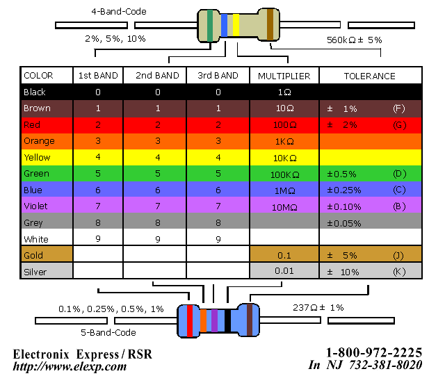
You can identify what value a resistor is by taking note of the coloured bands and turning them into calculations to figure out what value the resistor is. Each colour represents a number.


http://www.elexp.com/tips/clr_code.gif

To calculate the resistor shown above you compare the colour bands to the digits shown in the colour code chart. The first colour on the band gives you the first digit. The second band gives you the second digit and the third band gives you the digit of how many zeros you have to add to the calculation. So for example red is the first band and it represents 2, purple is the second digit to add which is 7, therefore the value so far is 27, and the third colour represents how many zero’s to add to the calculation which is yellow and yellow represents 4 so the value of the resistor will be 270000 ohms or 270k ohms. The fourth colour band represents the tolerance of the resistor. Gold makes one decimal place smaller 0.1 and silver makes two decimal places smaller 0.01 to the calculation.

below is a video of how to calculate resistor bands. I got this video off youtube.


http://www.youtube.com/watch?v=ab-enxLlYlU

Resistors in circuits:
You can connect the resistor in any way round. You can solder them and the heat won’t damage them. Resistance is measured in ohms and the symbol for ohms is an omega sign.


When resistors are connected in a series circuit the total resistance adds up to the individual resistances added together. For example Rt total resistance equals R1 + R2 + R3…


http://sub.allaboutcircuits.com/images/00087.png
The circuit above is of a series resistive circuit. To calculate the total resistance the formula Rt = R1 + R2 + R3 is used. Therefore Rt = 3000 + 10000 + 5000.
The combined resistance in a series circuit would always have a higher value than any of the individual resistors.

Resistors are identified in a circuit by the following pictures


Coils are not really used as resistors or to identify them in a circuit, but they do have resistance in them and they do get put in to calculations when working out the resistance in some circuits.


http://upload.wikimedia.org/wikipedia/commons/thumb/archive/f/f7/20070207122618!Resistor_symbol_GOST.svg/120px-Resistor_symbol_GOST.svg.png
This type of resistor symbol is commonly used.

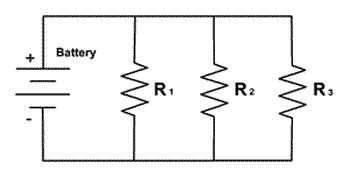
Resistors in parallel circuits are calculated different. The combined resistance in a parallel circuit will always have a lower value of resistance than any of the individual resistors. In this circuit resistors get there own voltage supply unlike in a series circuit each resistor has to divide the voltage. And if only 1 resistor is damaged and doesn’t conduct electrons in a parallel circuit then that is the only resistor that wouldn’t be working. But in a series circuit if only 1 resistor or component fails then the whole circuit would be open. 


Types of resistors


http://www.tpub.com/neets/book1/chapter1/1-29.gif


Above is a picture of different types of resistors and their symbols. 

Fixed carbon:
Depositing a carbon film onto a small ceramic cylinder makes this resistor. These types of resistors are most popular. 


Potentiometer type:


Below is a video of how a Potentiometer type resistor works. It is a video i got off Youtube.


http://www.youtube.com/watch?v=MXFvWLrpVSk

Hybrid Vehicles
A Hybrid vehicle is a vehicle that has an electric motor and a internal combustion engine connected in series or parallel to operate the vehicle.

How it works?
A Hybrid vehicle works like a normal vehicle when you first put the key in and start it up. The combustion engine creates energy for the vehicle to move until the engine warms up. When the vehicle stops at a traffic light when the engine is warmed up the electric motor turns on while the engine turns off which then means the engine uses less fuel saving the driver money and there would be no exhaust gases being created and coming out the tail pipe polluting the air. You can pull away and drive around at normal speeds using only electric power and if you want to pick up speeds the combustion engine will automatically turn on silently and smoothly and at that point the electric and engine will be running the vehicle. The electric motor will then turn off leaving only the combustion engine running for high speeds which also charges the electric motors battery.

Below is a video of how this type of hybrid vehicle works:


http://www.youtube.com/watch?v=2HrQeGzIZoI&feature=related

Tuesday 23 August 2011

Oxygen sensor circuit

Today in practical session we started working on building our next project, which is an oxygen sensor. The first step was to calculate the value of the resistors to go into the circuit.

Calculations

The first resistor I calculated using ohms law was R5. To get this value I had to use the formula R = V/A which is 12V – 0.6 (voltage drop across D2) – 9.1 (Zener-diode D1) equals 2.3v. The Amperage is shown on the sheet, which is 5.6mA that I have to convert to Amps so it would be 0.0056A. Therefore R = V/A = 2.3/0.0056 = 410.71 ohms. So for R5 I would use a resistor around this value.

The next resistor I calculated was R8. So R = V/A. the voltage I will be using is the voltage drop across this resistor and to work this out I had to minus 0.63v from 0.23v which were the available voltages before and after R8. Therefore the answer is 0.40v. The current is calculated using the formula A = V/R but before we can move on I have to calculate the current flow by using the values of R6. 9.1v is the available voltage before R6 and 0.63v is the available voltage after R6 (9.1 – 0.63 = 8.47v) so the voltage drop across this resistor is 8.47v, which is used for the voltage to calculate the current. The value of R6 is already known and is 10K. Therefore the current flow is A = V/R = 8.47/ 10000 = 0.000847A. So back to working out the value of R8 we now have the current to finish of the formula R = V/A. so 0.40/ 0.000847 = 472 ohms. So for R8 I will be using a resistor around this value.

To calculate the value of R7 I used the formula R = V/A. The available voltage is 0.23 before R7 and 0v after it so the voltage drop will be 0.23v and the current will be the same as R8, which is 0.000848A. So the value of R7 will be 0.23/0.000848 = 271ohms.

Now I will be calculating the values of R2, R3 and R4. So to calculate R2 I need to use R = V/A. First I need to work out my voltage I will be using and to do this I need to minus 0.6v which is the voltage drop across D2 IN4001 diode and 1.8v which is the voltage drop across LED1. I need to minus this from 12v so (0.6 + 1.8 – 12) = 9.6v. The current is already shown on the sheet and is 9.5mA that I have to convert to Amps which is then 0.0095A. So now I can calculate the value of R7. R = V/A = 9.6/0.0095 = 1010ohms.

The next resistor is R3. I will be using R = V/A to calculate its value. First I need to workout the voltage drop across this resistor. So there’s 12v coming in and 0.6v drops across D2 and another 0.6v drops across D4 and 1.8v drops across LED 5 and added up equals (0.6 + 0.6 + 1.8 – 12) = 9v. The current remains 9.5mA (0.0095A). So the value of R3 is R = V/A = 9/0.0095 = 947ohms. I don’t know if there is a 947ohm resistor, so Il be using the nearest 1 to this value which would probably be 1K or 1000ohms.

The final resistor to calculate is R4.  Its just like above were I have to add up the voltage drops before the resistor. So 12 – 0.6 + 1.8 = 9.6v.  The current is still the same in this part of the circuit, which is 9.5mA. Therefore R = V/A = 9.6/0.0095 = 1010ohms.

Component list

After calculating the values of R5, R8, R7, R2, R3 and R4 I had to show the tutor my workings of how I got these values. Once the tutor checked it I then moved on to build the circuit on a breadboard. The components I used are

Three 1N4001 Rectified diodes for D2, D3 and D4, according to the relevant data sheet these diodes have a maximum Pd of 2.5W, max current is 1A  @ 75°C and max reverse voltage of 100V.

One 9v1 zener diode for D1

Two 0.1 uF capacitors for C1 and C2

Three LED’s, one red for LED1 (I will use this to show when I’m running lean), one yellow for LED5 (to show when I’m running in between lean and rich) and one green for LED6 (for when I’m running rich or when accelerating because green represents GO)

A 380ohm resistor for R5
A 10,000 or 1Kohm resistor for R6
A 470ohm resistor for R8
A 270ohm resistor for R7

Wires


Op Amp


Below are pictures of the circuit i built on bread board:


After building this circuit on bread board i then tested it and it worked. I will go into more detail with a video i will be recording next week because i had no time in class to do it on friday. I also finished building this circuit on the green board which I still need time to record a video and show how the circuit works. But for now I will include a topic from ''subjects to study'' from moodle to add to my blog.


Zener Diodes

A zener diode is just like a normal rectifying diode that only allows current to flow in one direction from anode to cathode (forward bias) when a voltage of 0.6v is reached to open the gate and allow electrons to flow. But with a zener diode current can also flow in reverse direction (reverse bias) when the voltage is above a certain value, for example 6volts. This is called the break down voltage known as the zener voltage.

A zener diode can be used to make a simple voltage regulation circuit. The output voltage is fixed at the zener voltage of the zener diode used and so can be used to power devices requiring a fixed voltage. If you have a regulated fixed voltage - say 12 Volts from a power supply, and you want to power something requiring a lower voltage, it is possible to simply place a zener diode in series with the load device. You would choose a diode with a zener voltage equal to the supply voltage minus the voltage drop across the load.

For example, if you have a 1W 6V lightbulb to power from a 12 Watt regulated power supply, a 6.2V zener diode could be placed in series with the bulb giving the bulb 5.8V, or you could overpower the bulb a little using a 5.6V zener diode and dropping 6.4V across the bulb. Heat would be generated in the zener diode so it is essential to calculate the power lost in it so a suitably rated diode could be chosen.

Below is a picture of a zener diode I got of the internet.


http://www.reuk.co.uk/What-is-a-Zener-Diode.htm


Saturday 20 August 2011

Injector circuit.

In practical class today we got handed a sheet with an injector circuit that we had to calculate what value resistors we had to put in the circuit and what the available voltage and voltage drop would be after each
component. We also had to find out how much current flow there will be going through the diodes and transistors and check that reading with the data sheet to make sure we don't exceed the maximum values.

Component list

The components I used in creating this circuit were calculated first on a piece of paper we got handed. Ill show why I picked these particular components under my next heading Calculations. So I used four 470 ohm resistors, two 1N4001or 7 Light Emitting Diode’s and two Bipolar Junction NPN BC547 transistors. I built this circuit first on a breadboard shown in the picture below. 


After building the circuits on breadboards we used a software tool on the computer called Loch master 3.0 were we practiced making the injector circuits on PCB boards. It includes all components al l we had to do was select what component we needed then soldered it to the board. The good thing about this tool is that it allows you to practice building a circuit on the computer were you could easily change things around and figure out were your going to solder the component so that its tidy and evenly spaced so that everything fits properly. After designing the circuit on the computer we used it to build it on an actual board made with copper strips in lines to conduct electricity. The boards are about 50 x 40mm long with holes to insert components to solder. Below is a picture of my board I designed on loch master


Technical explanation of how this circuit works:

Resistors R1 and R3 have one leg connected to a 12v supply and the other leg to the anode side of LED’s D1 and D2 were a voltage drop of .6v is used to turn the led’s on. The cathode probes are connected to the collector terminals of the transistors. R2 and R4 are resistors connected to a 5v modulator, which acts as the ECU sending output pulses to the LED’s, which are meant to be the injectors. In creating this circuit I had to make cuts in between resistors R2 and R4 so voltage can be divided through the resistors to allow a current flow to the base terminals of the transistors. Both the emitter terminals are connected to earth.


This picture shows what it looks like on the other side of the board were soldering the components is done.  


I then made this circuit on to a pcb board.


Calculations

The PD across LED’s 1N4007 is calculated using the formula, pd = ID x VD and A = V/R from ohms law. This formula is used to see if we can use the type of resistor for this diode so that it doesn’t damage the LED.  LED’s have no resistance in them so it important to use the right resistor.

First the amperage flow must be calculated through the LED.
I = V/R therefore voltage is 12 – 0.6 / 470 = 11.4/470 = 0.02A
So now that I have amperage flow I can use this to calculate the power rating of the diode and check with the data sheet if it can handle this amount. Therefore Pd = ID X VD = 0.02 x 0.6 = 0.12 W
According to the data sheet for this led the total device dissipation above 25°C is 2.5W and the average current is 1.0A @ TA 75°C. 

Below is a video of my injector circuit connected to a 12v supply and a 5v modulator connected to the base of the transistor to show how the ecu will change the frequency of the pulse width of the injectors, in this case the LED's. In a car if i started to accelerate the ecu will send signals to the injectors and the injectors will spray at whatever signal they receive from the driver. In my video below i change the frequency high and low which in turn changes how the LED's flash. As i increase the frequency the led's start flashing faster and faster until i have fully increased it, and at this point the LED's stay constantly on and you cant really see them flashing only a tiny but if you look hard. 


Reflection


In making my injector circuit if i had the opportunity to make it again i will and make it better. I will spend more time on loch master designing my circuit so that it looks more professional when I make it. On the other hand I had a fair idea of how the injectors will spray by watching how the LED's flashed. 


Sunday 14 August 2011

EXPERIMENT No.8


EXPERIMENT No. 8

Summary: Vary the base resistor and measure changes in voltage and current for Vce, Vbe, Ic, and Ib. Then plot a load line.


Set up the following circuit on a bread board. Use a 470R for Rc and a BC547 NPN transistor.


Pick five resistors between 2K2 and 1M for Rb. You want a range of resistors that allow you to see Vce when the transistor is the saturated switch region and when it is in the active amplifier region. I used 47K, 220K, 270K, 330K and 1M, but this can vary depending on your transistor. Some may need to use 2K2. Put one resistor in place, and measure and record voltage drop across Vce and Vbe. Also measure and record the current for Ic and Ib. Then change the Rb resistor and do all the measurements and record the new readings. Do this for each of the resistor values above.


  Record here:
            Rb 47K            Vbe 0.69V       Vce 0.08V       Ib 0.02mA        Ic 6.41mA
Rb 220K          Vbe: 0.67V      Vce: 0.15V      Ib: 0.03mA       Ic: 6.24mA
Rb 270K          Vbe: 0.69V      Vce: 0.20V      Ib: 0.03mA       Ic: 6.21mA
Rb 330K          Vbe: 0.67V      Vce: 0.30V      Ib: 0.03mA       Ic: 6.01mA
Rb _____         Vbe: _____     Vce: _____     Ib: _____         Ic: _____

Your voltage drop measurements across Vce should vary from below 0.3 v (showing the transistor is in the saturated switch region) to above 2.0 v (showing the transistor is in the active amplifier region) If this is not the case, you may have to try a smaller or bigger resistor at Rb. Talk to your teacher to get a different size resistor, and redo your measurements.


 Discuss what happened for Vce during this experiment. What change took place, and what caused the change? 


During this experiment the different resistors caused different voltage drop readings at collector to emitter (Vce). The base resistors take up most of the voltage, which is 4.3 volts and the supply voltage is 5 volts. So the base resistors (Rb) take up 4.3 volts, so the voltage are low at 'Vce'...

Discuss what happened for Vbe during this experiment. What change took place if any, and what caused the change?


During this experiment the voltage at base to emitter (Vbe) got around .7 of a volt like a diode in its forward bias of 0.7 volt drop across it. So the resistors took up 4.3 volts and 0.7 volt remaining is used to push current from the base to emitter. So the resistors voltage and the voltage - base to emitter added up to the supply voltage which was 5 volts.

Discuss what happened for Ib during this experiment. What change took place, and what caused the change?

 Discuss what happened for Ic during this experiment. What change took place, and what caused the change? 

Plot the points for Ic and Vce on the graph below to create a load line. Plan the values for so you use up the graph space.  Use Ic as your vertical value, and Vce as your horizontal value.
Using Vbe on the Vce scale, plot the values of Ib so the finished graph looks similar to fig 13


Calculate the Beta (Hfe) of this transitor using the above graph.
  
 Explain what the load line graph is telling you. Discuss the regions of the graph where the transistor is Saturated, Cut-off, or in the Active area. 

EXPERIMENT No.7


EXPERIMENT No. 7

Transistor as a switch

Components: 1 x Small Signal NPN transistor, 2 resistors.

Exercise:  Connect the circuit as shown in Fig 12 and switch on the power supply.


Fig 12


Connect the multimeter between base and emitter.
Note the voltage reading and explain what this reading is indicating.

The voltage between base and emitter is 0.8v which is the voltage required to push electric charge through the insulating layer from the base to emitter. A small current appears.

Connect the multimeter between collector and emitter.
Note the voltage reading and explain what this reading is indicating.

The voltage between collector and emitter is 0.6v which means the base has free holes for the electrons to move along and are closer so you don’t need a higher voltage like .8v to move electrons. A higher current appears (20mA) because electrons can move/flow easier.

In the plot given below what are the regions indicated by the arrows A & B?


Fig 13
How does a transistor work in these regions? Explain in detail:

A – Cutoff = Transistors that are fully off
B - Saturated = Transistors that are fully on

What is the power dissipated by the transistor at Vce of 3 volts?
P= I x V
   =15 x 2.7
   =15mA x 2.7(Vce)
   =0.4micro W / 400 mW
   =0.0405 Watts

What is the Beta of this transistor at Vce 2,3 & 4 volts?

2Vce - B=Ic/Ib = 20mA/0.8mA = 25
3Vce - B=Ic/Ib = 15mA/0.6mA = 25
4Vce - B=Ic/Ib = 5mA/0.2mA = 25


EXPERIMENT No.6 Meter check of a transistor


EXPERIMENT No. 6


Meter check of a transistor

Bipolar transistors are constructed of a three-layer semiconductor “sandwich,” either PNP or
NPN. As such, transistors register as two diodes connected back-to-back when tested with a
multimeter’s  “diode check” function as illustrated in Figure 9.1. Low voltage readings on the base with the black negative (-) leads correspond to an N-type base in a PNP transistor. On the symbol, the N-type material corresponds to the “non-pointing” end of the base-emitter junction, the base. The P-type emitter corresponds to “pointing” end of the base emitter junction the emitter.


9.1: PNP transistor meter check: (a) forward B-E, B-C, voltage is low; (b) reverse
B-E, B-C, voltage is OL.


BIPOLAR JUNCTION TRANSISTORS
Here I’m assuming the use of a multimeter has a diode test function to check the PN junctions.
If your meter has a designated “diode check” function, and the meter will display the actual forward voltage of the PN junction and not just whether or not it conducts current.
Meter readings will be exactly opposite, of course, for an NPN transistor, with both PN
junctions facing the other way.
 Low voltage readings with the red (+) lead on the base is the “opposite” condition for the NPN transistor. If a multimeter with a “diode check” function is used in this test, it will be found that
the emitter-base junction possesses a slightly HIGHER forward voltage drop than the collector
base junction. This forward voltage difference is due to the disparity in doping concentration
between the emitter and collector regions of the transistor; the emitter is a much more heavily
doped piece of semiconductor material than the collector, causing its junction with the base to
produce a higher forward voltage drop.
Knowing this, it becomes possible to determine which terminal is which on an unmarked transistor.
This is important because transistor packaging, unfortunately, is not standardised. All
bipolar transistors have three terminals, of course, but the positions of the three terminals on the actual physical package are not arranged in any universal, standardised order.
Suppose a technician finds a bipolar transistor and proceeds to measure voltage drop with a
multimeter set in the “diode check” mode. Measuring between pairs of terminals and recording the
values displayed by the meter, the technician obtains the data in Figure 9.2.


Figure 9.2: Unknown bipolar transistor. Which terminals are emitter, base, and collector?
-meter readings between terminals.

The only combinations of test points giving conducting meter readings are terminals 1 and 3
(red test lead on 1 and black test lead on 3), and terminals 2 and 3 (red test lead on 2 and black test lead on 3). These two readings must indicate forward biasing of the emitter-to-base junction
(0.655 volts) and the collector-to-base junction (0.621 volts).
Now we look for the one terminal common to both sets of conductive readings. It must be the
base connection of the transistor, because the base is the only layer of the three-layer device
common to both sets of PN junctions (emitter-base and collector-base). In this example, that
terminal is number 3, being common to both the 1-3 and the 2-3 test point combinations.

METER CHECK OF A TRANSISTOR
Those sets of meter readings, the black (-) meter test lead was touching terminal 3, which tells us
that the base of this transistor is made of N-type semiconductor material (black = negative).
Thus, the transistor is a PNP with base on terminal 3, emitter on terminal 1 and collector on terminal 2 as described in Figure 9.3.


·       E and C reverse: 1(+) and 2(-): “OL”

·       E and C reverse: 1(-) and 2(+): “OL”

·       E and B forward: 1(+) and 3(-): 0.655 V

·       E and B forward: 1(-) and 3(+): “OL”

·       C and B forward: 2(+) and 3(-): 0.621 V

·       C and B forward: 2(-) and 3(+): “OL”

Figure 9.3: BJT terminals identified by meter.

Please note that the base terminal in this example is not the middle lead of the transistor, as one
might expect from the three-layer “sandwich” model of a bipolar transistor. This is quite often
the case, and tends to confuse new students of electronics. The only way to be sure which lead
is which is by a meter check, or by referencing the manufacturer’s “data sheet” documentation
on that particular part number of transistor.


Knowing that a bipolar transistor behaves as two back-to-back diodes when tested with a
Diode test function is helpful for identifying an unknown transistor purely by meter readings.
It is also helpful for a quick functional check of the transistor. If the technician were to measure
Using the Diode test function in any more than two or any less than two of the six test lead combinations, he or she would immediately know that the transistor was defective (or else that it wasn’t a bipolar transistor but rather something else – a distinct possibility if no part numbers can be referenced for sure identification!). However, the “two diode” model of the transistor fails to
explain how or why it acts as an amplifying device.


                                                                   Fig 10
Identify the legs of your transistor with a multimeter. For identifying and testing purposes, refer to the representation shown above.

Diode test (V) meter readings
Transistor number
VBE
VEB
VBC
VCB
VCE
VEC
NPN
.841
0
.836
0
0
0
PNP
0
.892
0
.886
0
0